Give step-by-step solution with explanation and final answer:5. (5 points) Apply bubble pushing to redraw the circuit below, so it only contains inverters, NOR gates, and NAND gates. Explain when and where you add bubbles.
Question:
Give step-by-step solution with explanation and final answer: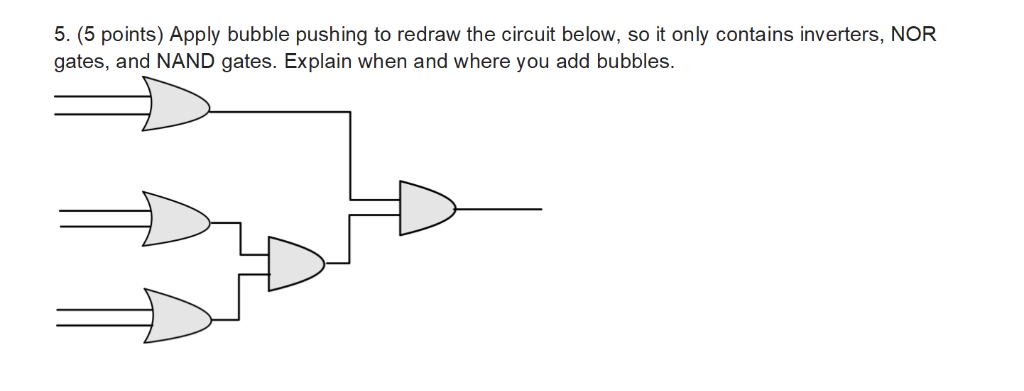 5. (5 points) Apply bubble pushing to redraw the circuit below, so it only contains inverters, NOR
gates, and NAND gates. Explain when and where you add bubbles.
5. (5 points) Apply bubble pushing to redraw the circuit below, so it only contains inverters, NOR
gates, and NAND gates. Explain when and where you add bubbles.
This is AI generated Response.
Asked by: M Raju
Created at: 2025-09-09 05:50:33
Asked by: M Raju
Created at: 2025-09-09 05:50:33
Final Answer:
Rendered
Raw Text
Did you like this answer?
Let's break down the step-by-step solution using bubble pushing, so the circuit **only contains inverters, NOR, and NAND gates**.
---
### **Step 1: Identify the Gates**
Looking at the circuit:
- The top three gates are **OR gates** (curved input side).
- The bottom-most gate is an **AND gate** (flat input side).
- The final gate (on the right) is an **AND gate**.
---
### **Step 2: Write the Boolean Expression**
Let's assign variables:
- Top: \( A, B \)
- Middle: \( C, D \)
- Bottom: \( E, F \)
The circuit is:
- \( X_1 = A + B \) (OR)
- \( X_2 = C + D \) (OR)
- \( X_3 = E + F \) (OR)
- \( X_4 = X_2 \cdot X_3 \) (AND)
- Output = \( X_1 \cdot X_4 \) (AND)
So the expression is:
\[
(A+B) \cdot ((C+D) \cdot (E+F))
\]
---
### **Step 3: Apply Bubble Pushing**
We want to replace OR and AND with NOR, NAND, and inverters only.
#### **a) Replace OR gates**
An OR gate can be written using NOR (with bubble pushing):
\[
A + B = \overline{ \overline{A + B} }
\]
- The inner part is a **NOR gate**.
- The outer bar is an **inverter**.
So, each OR gate becomes a NOR gate followed by an inverter.
#### **b) Replace AND gates**
Similarly, an AND gate can be written using NAND:
\[
A \cdot B = \overline{ \overline{A \cdot B} }
\]
- The inner part is a **NAND gate**.
- The outer bar is an **inverter**.
So, each AND gate becomes a NAND gate followed by an inverter.
---
### **Step 4: Redraw the Circuit with NOR, NAND, and Inverters**
#### **a) Rewrite Each Gate**
- **Each OR gate**: Replace with NOR + inverter.
- **Each AND gate**: Replace with NAND + inverter.
#### **b) Add Bubbles (Push Bubbles)**
- A bubble at the output of a gate means negation (inverter).
- When you push a bubble from the output to the inputs, you must also invert the gate type (DeMorgan's Law):
- \(\overline{A \cdot B} = \overline{A} + \overline{B}\) (NAND becomes NOR with inverted inputs)
- \(\overline{A + B} = \overline{A} \cdot \overline{B}\) (NOR becomes NAND with inverted inputs)
---
#### **Circuit step-by-step after bubble pushing:**
1. **Replace all OR gates with NOR gates, followed by inverters.**
- Each OR output gets a bubble (inverter).
2. **Replace all AND gates with NAND gates, followed by inverters.**
- Each AND output gets a bubble (inverter).
3. **Push bubbles towards the inputs as much as possible.**
- When two bubbles meet (inverter followed by inverter), they cancel out.
---
#### **Final Circuit:**
Let's label the outputs of each NOR/NAND gate:
- **Top:** \(\overline{A+B}\) (NOR gate) → inverter → \(A+B\)
- **Middle:** \(\overline{C+D}\) (NOR gate) → inverter → \(C+D\)
- **Bottom:** \(\overline{E+F}\) (NOR gate) → inverter → \(E+F\)
- **AND of middle and bottom:** Now, instead of AND, use NAND + inverter:
- NAND: \(\overline{(C+D) \cdot (E+F)}\)
- Inverter: \((C+D) \cdot (E+F)\)
- **Final output:** AND of \(A+B\) and \((C+D) \cdot (E+F)\):
- NAND: \(\overline{(A+B) \cdot ((C+D) \cdot (E+F))}\)
- Inverter: \((A+B) \cdot ((C+D) \cdot (E+F))\)
---
### **Step 5: Draw the Final Circuit**
Here is your circuit, using only NOR, NAND, and inverters:
```
A---| | |>o---| | | |
|NOR |---o-----| INV | | |
B---|____| | ____| | |
| | | |
C---| | | |--|NAND|---| INV |
|NOR |---| | |_____| | |
D---|____| | | | |
| | | |
E---| | | | | |
|NOR |---| | | |
F---|____| | | | |
| | | |
|-------------o------------| |
|
-----------------------------------------------------o---|NAND|---|INV|---OUTPUT
```
#### **Where and When Bubbles are Added:**
- After every NOR or NAND, add an inverter (bubble) at the output.
- When connecting to the next gate, if you see two inverters in a row, remove both (they cancel).
- Each original OR is now a NOR + inverter.
- Each original AND is now a NAND + inverter.
---
### **Conclusion**
**Final answer:**
By bubble pushing and applying DeMorgan's laws, you can redraw the circuit **using only NOR, NAND, and inverters**.
- Replace every OR with a NOR + inverter.
- Replace every AND with a NAND + inverter.
- Push bubbles (inverters) as far toward the inputs as possible, canceling double inverters when they appear.
If you want a hand-drawn version or step-by-step drawing, let me know!
📢 Instructions:
- Ask anything relatd to above question only.
- For new Question goto :