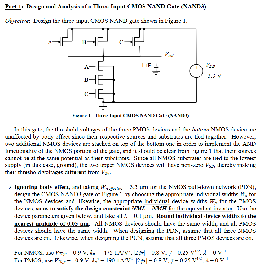
Give step-by-step solution with explanation and final answer:Part 1: Design and Analysis of a Three-Input CMOS NAND Gate (NAND3)
Objective: Design the three-input CMOS NAND gate shown in Figure 1.
5 oO
5 33V
cÔÇö Cc]
Figure 1. Three-Input CMOS NAND Gate (NAND3)
In this gate, the threshold voltages of the three PMOS devices and the bottom NMOS device are
unaffected by body effect since their respective sources and substrates are tied together. However,
two additional NMOS devices are stacked on top of the bottom one in order to implement the AND
functionality of the NMOS portion of the gate, and it should be clear from Figure 1 that their sources
cannot be at the same potential as their substrates. Since all NMOS substrates are tied to the lowest
supply (in this case, ground), the two upper NMOS devices will have non-zero Fs, thereby making
their threshold voltages different from Vz.
= Ignoring body effect, and taking W,,egcve = 3.5 jim for the NMOS pull-down network (PDN),
design the CMOS NANDS3 gate of Figure 1 by choosing the appropriate individual widths 77, for
the NMOS devices and, likewise, the appropriate individual device widths #7 for the PMOS
devices, so as to satisfy the design constraint NML = NMH for the equivalent inverter. Use the
device parameters given below, and take all Z = 0.1 pm. Round individual device widths to the
nearest multiple of 0.05 pm. All NMOS devices should have the same width, and all PMOS
devices should have the same width. When designing the PDN, assume that all three NMOS
devices are on. Likewise, when designing the PUN, assume that all three PMOS devices are on.
For NMOS, use Vr = 0.9 V, kyÔÇÖ = 475 LA/V2, [24 = 0.8 V, y= 025 V2, 2=0 VL.
For PMOS, use Vg, =ÔÇö0.9 V, k,ÔÇŁ = 190 pA/V?, 2: = 0.8 V, y= 025 VIZ 1=0 Vv"
Question:
Give step-by-step solution with explanation and final answer:Part 1: Design and Analysis of a Three-Input CMOS NAND Gate (NAND3)
Objective: Design the three-input CMOS NAND gate shown in Figure 1.
5 oO
5 33V
cÔÇö Cc]
Figure 1. Three-Input CMOS NAND Gate (NAND3)
In this gate, the threshold voltages of the three PMOS devices and the bottom NMOS device are
unaffected by body effect since their respective sources and substrates are tied together. However,
two additional NMOS devices are stacked on top of the bottom one in order to implement the AND
functionality of the NMOS portion of the gate, and it should be clear from Figure 1 that their sources
cannot be at the same potential as their substrates. Since all NMOS substrates are tied to the lowest
supply (in this case, ground), the two upper NMOS devices will have non-zero Fs, thereby making
their threshold voltages different from Vz.
= Ignoring body effect, and taking W,,egcve = 3.5 jim for the NMOS pull-down network (PDN),
design the CMOS NANDS3 gate of Figure 1 by choosing the appropriate individual widths 77, for
the NMOS devices and, likewise, the appropriate individual device widths #7 for the PMOS
devices, so as to satisfy the design constraint NML = NMH for the equivalent inverter. Use the
device parameters given below, and take all Z = 0.1 pm. Round individual device widths to the
nearest multiple of 0.05 pm. All NMOS devices should have the same width, and all PMOS
devices should have the same width. When designing the PDN, assume that all three NMOS
devices are on. Likewise, when designing the PUN, assume that all three PMOS devices are on.
For NMOS, use Vr = 0.9 V, kyÔÇÖ = 475 LA/V2, [24 = 0.8 V, y= 025 V2, 2=0 VL.
For PMOS, use Vg, =ÔÇö0.9 V, k,ÔÇŁ = 190 pA/V?, 2: = 0.8 V, y= 025 VIZ 1=0 Vv"
This is AI generated Response.
Asked by: M Murali
Created at: 2025-11-02 20:45:26
Final Answer:
RenderedRaw Text
Did you like this answer?
Let's break down the solution step-by-step for designing the **three-input CMOS NAND gate** by finding the required widths of the NMOS and PMOS devices, given the design constraint **NML = NM** for the equivalent inverter.
---
## **Step 1: Understanding the Problem**
- **NAND3 Gate**: 3 PMOS in parallel (pull-up), 3 NMOS in series (pull-down)
- **Design Goal**: Choose NMOS and PMOS widths so that the **Noise Margins** for Low and High are equal (**NML = NMH**).
- **Given**:
- \( W_{n, \text{effective}} = 3.5\,\mu m \)
- \( L = .1\,\mu m \)
- **NMOS parameters**:
- \( V_{T,n} = .9\,V \)
- \( k'_n = 475\,\mu A/V^2 \)
- \( |\phi_f| = .8\,V \)
- \( \gamma = .25\,V^{1/2} \)
- \( \lambda = \)
- **PMOS parameters**:
- \( V_{T,p} = -.9\,V \)
- \( k'_p = 190\,\mu A/V^2 \)
- \( |\phi_f| = .8\,V \)
- \( \gamma = .25\,V^{1/2} \)
- \( \lambda = \)
- \( V_{DD} = 3.3\,V \)
---
## **Step 2: Pull-Down Network (NMOS Stack)**
- **NMOS** stack of 3 devices in series.
- **Effective Width**: When stacking \( N \) NMOS devices, the effective width is \( W_n / N \).
- We are **given** \( W_{n, \text{effective}} = 3.5\,\mu m \) for the whole stack:
\[
W_n (\text{individual}) = N \times W_{n, \text{effective}} = 3 \times 3.5\,\mu m = 10.5\,\mu m
\]
- **Round to nearest .05 ╬╝m**: Already a multiple, so
\[
\boxed{W_n = 10.5\,\mu m}
\]
---
## **Step 3: Pull-Up Network (PMOS Parallel)**
- **3 PMOS devices in parallel**: Each PMOS sees the same \( V_{DS} \), so each device should have the same width.
- For **equivalent inverter**, the pull-up (PMOS) strength should match the pull-down (NMOS) stack.
- **Strength Ratio**:
\[
\text{Strength} = \mu_n C_{ox} \frac{W_n}{L} \quad \text{vs} \quad \mu_p C_{ox} \frac{W_p}{L}
\]
where \( \mu_n C_{ox} = k'_n \), \( \mu_p C_{ox} = k'_p \).
- **For equivalent inverter**:
\[
k'_n \frac{W_{n,\text{eff}}}{L} = k'_p \frac{W_{p,\text{total}}}{L}
\]
where \( W_{p,\text{total}} = 3 W_p \), \( W_p \) is width of each PMOS.
\[
k'_n W_{n,\text{eff}} = k'_p (3 W_p)
\]
\[
W_p = \frac{k'_n W_{n,\text{eff}}}{3 k'_p}
\]
Plug in values:
\[
W_p = \frac{475 \times 3.5}{3 \times 190}
\]
\[
W_p = \frac{1662.5}{570} \approx 2.9175\,\mu m
\]
**Round to nearest .05 ╬╝m:**
\[
W_p = 2.90\,\mu m
\]
---
## **Step 4: Final Answers**
- **NMOS width (each):** \( \boxed{10.5\,\mu m} \)
- **PMOS width (each):** \( \boxed{2.90\,\mu m} \)
---
### **Summary Table**
| Device | Number in Network | Individual Width (\(\mu m\)) | Length (\(\mu m\)) |
|--------|-------------------|------------------------------|--------------------|
| NMOS | 3 (series) | 10.5 | .1 |
| PMOS | 3 (parallel) | 2.90 | .1 |
---
## **Explanation**
- **NMOS widths**: Set so the *effective* width for 3 in series matches the inverter's value.
- **PMOS widths**: Set so the total pull-up strength (sum for 3 in parallel) matches the NMOS stack, using the ratio of \( k'_n \) and \( k'_p \).
---
## **Final Answer**
\[
\boxed{
\text{NMOS width (each): } 10.5\,\mu m \\
\text{PMOS width (each): } 2.90\,\mu m
}
\]
Let me know if you need the detailed device equations or further explanation!
Question:
Give me Each Step Exaplines in 50 Words Only Theory
This is AI generated Response.
Asked by: M Murali
Created at: 2025-11-02 20:47:59
Final Answer:
RenderedRaw Text
Did you like this answer?
# Step-by-Step Theory Explanation
## Step 1: Understanding the Problem
The objective is to design a three-input CMOS NAND gate (NAND3) with equal noise margins for low (NML) and high (NMH). The design requires dimensions for NMOS and PMOS devices, taking into account their electrical characteristics and the gate's stacking configuration.
## Step 2: Pull-Down Network (NMOS Stack)
In the NMOS stack, the effective width is divided among three devices in series. The total effective width is given as \(3.5\,\mu m\), leading to an individual width of \(10.5\,\mu m\). This ensures the NMOS can effectively pull down the output when all inputs are high.
## Step 3: Pull-Up Network (PMOS Parallel)
For the PMOS, which operates in parallel, an equivalent pull-up strength is calculated. The width of each PMOS device is determined using the ratio of NMOS to PMOS transconductance parameters. This results in an individual PMOS width of \(2.90\,\mu m\), satisfying the noise margin condition.
## Step 4: Final Answers
The final dimensions for the three-input CMOS NAND gate are \(10.5\,\mu m\) for each NMOS device and \(2.90\,\mu m\) for each PMOS device. These values ensure that the gate meets the design specifications of equal noise margins while maintaining proper functionality.
VIPSolutions focuses on clear, stepÔÇĹbyÔÇĹstep explanations so you can learn quickly. Whether you need an AIÔÇĹgenerated walkthrough or a short hint to get unstuck, each solution is organized for fast reading and easy review later.
Search similar questions, compare approaches, and bookmark the best answers for revision. Our goal is simple: quick, reliable study help that feels naturalÔÇönot noisy.
 Part 1: Design and Analysis of a Three-Input CMOS NAND Gate (NAND3)
Objective: Design the three-input CMOS NAND gate shown in Figure 1.
5 oO
5 33V
cÔÇö Cc]
Figure 1. Three-Input CMOS NAND Gate (NAND3)
In this gate, the threshold voltages of the three PMOS devices and the bottom NMOS device are
unaffected by body effect since their respective sources and substrates are tied together. However,
two additional NMOS devices are stacked on top of the bottom one in order to implement the AND
functionality of the NMOS portion of the gate, and it should be clear from Figure 1 that their sources
cannot be at the same potential as their substrates. Since all NMOS substrates are tied to the lowest
supply (in this case, ground), the two upper NMOS devices will have non-zero Fs, thereby making
their threshold voltages different from Vz.
= Ignoring body effect, and taking W,,egcve = 3.5 jim for the NMOS pull-down network (PDN),
design the CMOS NANDS3 gate of Figure 1 by choosing the appropriate individual widths 77, for
the NMOS devices and, likewise, the appropriate individual device widths #7 for the PMOS
devices, so as to satisfy the design constraint NML = NMH for the equivalent inverter. Use the
device parameters given below, and take all Z = 0.1 pm. Round individual device widths to the
nearest multiple of 0.05 pm. All NMOS devices should have the same width, and all PMOS
devices should have the same width. When designing the PDN, assume that all three NMOS
devices are on. Likewise, when designing the PUN, assume that all three PMOS devices are on.
For NMOS, use Vr = 0.9 V, kyÔÇÖ = 475 LA/V2, [24 = 0.8 V, y= 025 V2, 2=0 VL.
For PMOS, use Vg, =ÔÇö0.9 V, k,ÔÇŁ = 190 pA/V?, 2: = 0.8 V, y= 025 VIZ 1=0 Vv"
Part 1: Design and Analysis of a Three-Input CMOS NAND Gate (NAND3)
Objective: Design the three-input CMOS NAND gate shown in Figure 1.
5 oO
5 33V
cÔÇö Cc]
Figure 1. Three-Input CMOS NAND Gate (NAND3)
In this gate, the threshold voltages of the three PMOS devices and the bottom NMOS device are
unaffected by body effect since their respective sources and substrates are tied together. However,
two additional NMOS devices are stacked on top of the bottom one in order to implement the AND
functionality of the NMOS portion of the gate, and it should be clear from Figure 1 that their sources
cannot be at the same potential as their substrates. Since all NMOS substrates are tied to the lowest
supply (in this case, ground), the two upper NMOS devices will have non-zero Fs, thereby making
their threshold voltages different from Vz.
= Ignoring body effect, and taking W,,egcve = 3.5 jim for the NMOS pull-down network (PDN),
design the CMOS NANDS3 gate of Figure 1 by choosing the appropriate individual widths 77, for
the NMOS devices and, likewise, the appropriate individual device widths #7 for the PMOS
devices, so as to satisfy the design constraint NML = NMH for the equivalent inverter. Use the
device parameters given below, and take all Z = 0.1 pm. Round individual device widths to the
nearest multiple of 0.05 pm. All NMOS devices should have the same width, and all PMOS
devices should have the same width. When designing the PDN, assume that all three NMOS
devices are on. Likewise, when designing the PUN, assume that all three PMOS devices are on.
For NMOS, use Vr = 0.9 V, kyÔÇÖ = 475 LA/V2, [24 = 0.8 V, y= 025 V2, 2=0 VL.
For PMOS, use Vg, =ÔÇö0.9 V, k,ÔÇŁ = 190 pA/V?, 2: = 0.8 V, y= 025 VIZ 1=0 Vv"